
 Stock Surges 6% Following HBM4E Memory Chip Sample Delivery")
Key Highlights
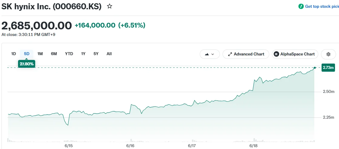
- Shares of SK Hynix climbed 6.51% following confirmation of HBM4E sample distribution to key industry partners
- The advanced 12-layer memory module achieves data transfer rates of 16Gbps per pin with power efficiency improvements exceeding 20%
- Utilizing Advanced MR-MUF manufacturing processes, the chip delivers 48GB storage capacity alongside a 17% boost in thermal management
- As Nvidia’s leading HBM provider, SK Hynix maintains its competitive edge over Samsung and Micron
- The chipmaker confirmed collaboration with industry partners to advance toward full-scale manufacturing
SK Hynix revealed Thursday that it has successfully delivered samples of its cutting-edge HBM4E memory technology to key industry customers, propelling the South Korean semiconductor manufacturer’s shares upward by 6.51% on the Korea Exchange. The announcement created ripple effects across the memory chip sector, with Samsung’s stock advancing 4.62% and Micron gaining 2.20%.
The newly developed HBM4E represents a 12-layer high-bandwidth memory solution specifically engineered for artificial intelligence workloads. The technology achieves maximum data throughput of 16 gigabits per second per pin while demonstrating power consumption improvements of over 20% when compared to the standard HBM4 variant.
High-bandwidth memory modules serve as critical infrastructure within AI processing units, including those manufactured by Nvidia. These components manage the massive data streams necessary for training and operating artificial intelligence systems. Their absence would render large-scale AI computing operations virtually impossible.
SK Hynix maintains its position as Nvidia’s principal HBM provider. While Samsung and Micron continue efforts to narrow the competitive divide, SK Hynix has sustained its market leadership across multiple technology iterations — spanning HBM3, HBM3E, and advancing through HBM4 to the current HBM4E generation.

The semiconductor manufacturer confirmed that the 12-stack HBM4E samples reached customers “on schedule,” attributing this achievement to its extensive expertise in HBM innovation and manufacturing capabilities that enabled meeting planned delivery dates.
Technical Advancements in HBM4E
The HBM4E architecture reduces data transmission delays through enhanced interface engineering and structural refinements, while maintaining operational stability under high-bandwidth conditions. This capability proves essential for AI datacenters managing continuous processing demands at enterprise scale.
SK Hynix employs a specialized production technique known as Advanced MR-MUF — Mass Reflow Molded Underfill — which introduces liquid protective compounds between layered chip components. This methodology enables the manufacturer to achieve 48GB capacity within a 12-layer configuration while enhancing thermal resistance by 17% compared to HBM4.
Enhanced thermal management characteristics ensure memory modules can function with greater reliability within high-performance computing environments that produce substantial heat output.
Path Toward Commercial Production
Ahn Hyun, serving as SK Hynix’s President and Chief Development Officer, stated the organization has “established a foundation to reinforce its AI dominance with HBM4E,” and confirmed plans to collaborate with industry partners for market delivery while preserving its status as a “comprehensive AI memory innovator.”
The company refrained from announcing a precise commercial production schedule, indicating only its commitment to “collaborate closely with partners for mass production in an appropriate timeframe.”
Nvidia’s shares declined 1.33% on Thursday, a movement not specifically connected to the SK Hynix disclosure.
The HBM4E sample distributions build upon SK Hynix’s proven history of delivering HBM3 and HBM3E solutions to the marketplace — earlier generations that solidified its strategic partnership with Nvidia prior to HBM4 development.