
 Stock: Memory Giant Commits $13B to New AI Chip Facility")
Key Highlights
- SK Hynix is committing 19 trillion won (approximately $13 billion) to construct a cutting-edge semiconductor packaging facility in South Korea.
- Dubbed P&T7, the installation will be situated in Heungdeok district within Cheongju and will specialize in sophisticated chip assembly operations.
- Groundbreaking scheduled for April 2026.
- The facility’s primary output will be high-bandwidth memory (HBM) components, essential for powering AI infrastructure and Nvidia’s processing systems.
- The memory manufacturer has already initiated volume production of cutting-edge memory solutions designed for Nvidia’s forthcoming Vera Rubin AI accelerator.
SK Hynix disclosed on Wednesday its intention to allocate approximately 19 trillion won — equivalent to about $13 billion — toward establishing a new state-of-the-art packaging manufacturing facility on South Korean soil. The production site, designated P&T7, will occupy space in Cheongju’s Heungdeok district.
According to regulatory documents, groundbreaking activities are scheduled to commence this month. This capital outlay represents one of the most substantial single-facility investments in the company’s history.
The production center will concentrate entirely on sophisticated packaging technologies — the critical procedures required to assemble high-bandwidth memory (HBM) components. HBM represents the memory architecture driving contemporary AI processing units, including those manufactured by Nvidia’s premium product lines.
SK Hynix ranks among the globe’s leading memory semiconductor producers and serves as a principal component supplier to Nvidia. Market appetite for its offerings has intensified dramatically as artificial intelligence infrastructure deployments expand worldwide.

The Strategic Importance of Advanced Packaging
Sophisticated packaging extends beyond mere assembly — it fundamentally dictates the velocity and performance efficiency of memory chip data transfers. For artificial intelligence computing tasks, this throughput capability proves absolutely essential.
HBM technology employs vertically stacked memory layers interconnected via microscopic vertical pathways. Executing this methodology accurately at production volumes requires both exceptional technical expertise and substantial capital resources.
The corporation indicated it has been advancing capacity expansion timelines to satisfy incoming order demand. Earlier in the current year, the company accelerated the launch of an additional memory semiconductor plant within South Korea for identical strategic reasons.
The proposed investment amount remains flexible and may adjust according to evolving market dynamics and corporate strategic priorities, SK Hynix clarified in its official filing.
Vera Rubin Memory Module Manufacturing Commences
Earlier this week, SK Hynix revealed it had begun volume manufacturing of an advanced-generation memory solution engineered exclusively for Nvidia’s Vera Rubin AI processor — representing Nvidia’s subsequent platform generation following Blackwell.
This production announcement arrived mere days ahead of the $13 billion facility disclosure, emphasizing the aggressive pace at which the organization is advancing to cement its supply chain positioning.
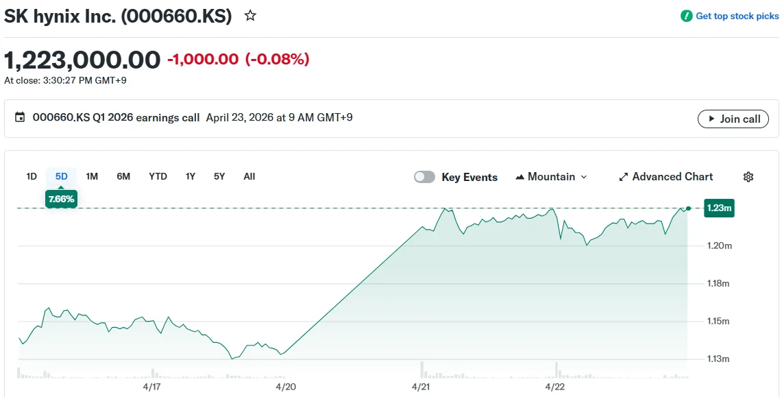
Shares declined approximately 1% on Wednesday in response to the investment revelation. This downturn followed a session where the stock had climbed to unprecedented peak valuations.
As of Wednesday’s trading, SK Hynix maintains a listing on the Korea Exchange under ticker symbol 000660. The manufacturer has not yet published a target completion timeline for the P&T7 installation.