
 Stock Surges 9% After Reports of New AI Chip Packaging Facility")
Key Takeaways
- Shares of Samsung Electronics climbed nearly 9% following reports the tech giant is planning to construct an advanced semiconductor packaging facility in Gwangju, South Korea.
- The potential investment announcement may come during a June 29 summit between South Korean President Lee Jae Myung and top executives from the nation’s largest corporations.
- The proposed plant would strengthen Samsung’s position in advanced chip packaging technology, crucial for AI semiconductor production.
- Samsung is locked in competition with SK Hynix for dominance in the high-bandwidth memory sector, serving clients like Nvidia, AMD, and Google.
- Samsung recently started delivering prototype units of its newest 12-layer HBM4E memory chip to clients in May.
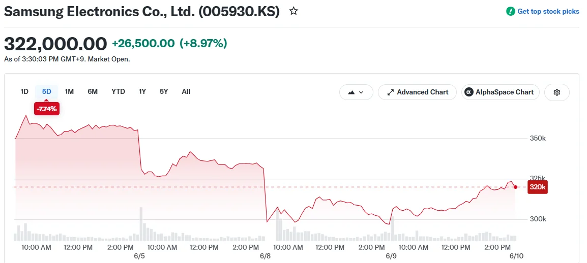
Shares of Samsung Electronics (005930) surged nearly 9% during Tuesday’s trading session after the Korea Economic Daily published a report indicating the company is evaluating plans to establish an advanced semiconductor packaging plant in Gwangju, located in southwestern South Korea.
According to the publication, which referenced unnamed industry insiders, Samsung may unveil this investment initiative at an upcoming June 29 summit hosted at the presidential residence. The meeting will bring together South Korean President Lee Jae Myung and executives from the country’s most prominent business conglomerates.
Samsung Electronics Chairman Jay Y. Lee is anticipated to participate in the event, alongside SK Group Chairman Chey Tae-won. The presidential gathering centers on the theme of implementing a “major shift in growth strategy” for South Korea’s corporate sector.
Samsung has not issued any official statement regarding the report. Meanwhile, representatives from the presidential office noted that capital investment choices remain within the purview of individual corporations.

The Strategic Importance of Advanced Packaging
Advanced semiconductor packaging has emerged as a critical competitive arena within the chip manufacturing industry. This technology enables manufacturers to vertically stack and combine multiple silicon dies within a single package unit, enhancing computational performance without depending exclusively on traditional transistor miniaturization.
Demand has surged particularly for high-bandwidth memory solutions. HBM technology vertically stacks several DRAM chips and works in tandem with AI processors manufactured by companies such as Nvidia. These memory components are essential infrastructure for AI-powered servers.
Samsung currently provides semiconductor solutions to leading AI technology firms including Nvidia, AMD, and Google — companies that are collectively driving unprecedented demand for sophisticated memory products deployed in artificial intelligence data centers.
The establishment of a new packaging facility in Gwangju would represent Samsung’s effort to accelerate capital deployment in anticipation of a projected semiconductor industry upturn driven by artificial intelligence applications.
The Samsung-SK Hynix Rivalry
Samsung continues its efforts to narrow the competitive gap with SK Hynix, which currently holds the leading market position in the HBM segment. Interestingly, SK Hynix shares also experienced strong gains on Tuesday, climbing more than 15%.
Last month, Samsung announced it had commenced shipping evaluation samples of its most advanced HBM chip — the 12-layer HBM4E — to client companies. This represents a generational advancement from its predecessor models and demonstrates the company’s aggressive approach to maintaining competitive relevance.
The scheduled June 29 presidential meeting with conglomerate leadership could provide the formal platform for Samsung to publicly outline its strategic investment roadmap.
It’s important to note that Samsung has not officially validated the Gwangju facility plans, and the Korea Economic Daily’s report depends on anonymous industry sources for its information.